
 Crystals 11.jpg)
| Code | Size | Thickness | Orientation | Surface Finish | Unit Price | Delivery | Cart |
|---|---|---|---|---|---|---|---|
| 6505-001 | 10x10mm | 0.5mm | C-plane | SSP | Inquire | 2 weeks | |
| 6505-002 | 10x10mm | 0.5mm | C-plane | DSP | Inquire | 2 weeks | |
| 6505-003 | Φ12.7mm | 0.5mm | C-plane | SSP | Inquire | 2 weeks | |
| 6505-004 | Φ12.7mm | 0.5mm | C-plane | DSP | Inquire | 2 weeks | |
| 6505-005 | Φ25.4mm | 0.5mm | C-plane | SSP | Inquire | 2 weeks | |
| 6505-006 | Φ25.4mm | 0.5mm | C-plane | DSP | Inquire | 2 weeks | |
| 6505-007 | φ50.8mm | 0.43mm | C-plane | SSP | Inquire | 2 weeks | |
| 6505-008 | φ50.8mm | 0.4mm | C-plane | DSP | Inquire | 2 weeks | |
| 6505-009 | φ100mm | 0.65mm | C-plane | SSP | Inquire | 2 weeks | |
| 6505-010 | φ100mm | 0.5mm | C-plane | DSP | Inquire | 2 weeks | |
| 6505-011 | φ150mm | 1.0mm | C-plane | SSP | Inquire | 2 weeks | |
| 6505-012 | φ150mm | 1.0mm | C-plane | DSP | Inquire | 2 weeks |
Sapphire is an excellent substrate material for the epitaxial growth of various thin films. Sapphire has exceptional high-temperature resistance, chemical corrosion resistance, electrical insulation, wide optical transmission, unrivaled mechanical hardness, and wear resistance. The molecular bonding of sapphire is strong, enabling the production of thinner pieces without fracture.
Sapphire Wafers and Substrates are versatile, their uses include but are not limited to III-V and II-VI compound thin film growth for semiconductor, Light Emitting Diodes(LEDs), Y-series, La-series high temperature superconducting (HTSC) thin films, Microelectronic IC (Silicon on Sapphire Integrated Circuit, SOS), Hybrid Microelectronic applications, and ferromagnetic/ferroelectric thin film growth.
A-plane Sapphire Substrates and Wafers are suitable alternatives for Hybrid Microelectronic applications, which mainly include HIC and MCM, due to their uniform dielectric constants and high electrical insulations. TlBaCaCuO (TbBaCaCuO), Tl-2212, the hetero-epitaxial superconducting thin film could grow with success on an a-plane sapphire cerium oxide (CeO2) composite substrate to obtain angstrom level surface finishes.
Whilst R-plane Sapphire Substrates and Wafers find great usage in the hetero-epitaxial deposition of silicon for Microelectronic IC (High-Speed Silicon On Sapphire, SOS).
C-plane Sapphire Substrates and Wafers are also the mainstream options to perform the Metal Organic Chemical Vapor Deposition (MOCVD) growth of a series of III-V and II-VI compound thin films beside GaN, such as AlN, AlGaN, and InGaN to manufacture current blue, violet, and white light-emitting diodes (LEDs), and blue laser diodes (LDs). Another aptness of c-plane sapphire is the growth of ferroelectric thin films. (Pb,La)(Zr,Ti)O3 (PLZT) ferroelectric thin films grown using rf‐planar magnetron sputtering on C-plane sapphire is also one of the candidates worth noticing to manufacture new functional electronics. When assign to the sputter deposition of Pb(Zr,Ti)O3 (PZT) ferroelectric thin films, sapphire substrates show a lower degree of disorientation between the crystallites compared to on Si substrate and ideal breakdown voltage.
M-Plane Sapphire Substrates and Wafers could be competent in the ferromagnetic thin film growth of Mn1−xS (e.g. LP-MOCVD growth of MgxZn1-xO in solar-blind ultraviolet detection), pulsed laser deposition of Cr2O3 and other cobalt, Mn5Ge3Cx, etc. too.
Shanghai North Optics offers off-the-shelf and custom sapphire substrates and wafers for epitaxial thin film growth. North Optics has eminent capabilities and endeavors to produce high-precision sapphire wafers. We select single crystal sapphire with superior sapphire purities to fabricate the wafers and substrates. A series of advanced equipment is utilized to manufacture our products in a class 1000 clean room. Before shipment, we conduct XRD diffraction analysis and use Atomic Force Microscope (AFM) (See the reports in the technical imaging section) to inspect the product to ensure optimum surface qualities of the product. The standard versions have a c-plane orientation, whilst other orientations including a-plane, r-plane, and m-plane are also available. The maximum diameter is 6 inches, and substrates could either be single-side polished or double-side polished. In addition to the standard circular shapes, other shapes like square and rectangular are also available.
Common Specifications:
| Materials | Al2O3 crystals or sapphire | Orientation Error | ±0.5deg. |
| Orientation | A-plane | <11-20> | 2.379Å |
| R-plane | <1-102> | 1.740Å | |
| M-plane | <10-10> | 1.375Å | |
| C-plane | <0001> | 2.165Å | |
| Maximum Diameter | 6 inches | Surface Finish | SSP (single surface polished) or DSP (double surface polished) |
Basic Properties:
| Crystal Structure | Hexagonal | Unit Cell Constant | a=4.748Å c=12.97Å |
| Melt Point(℃) | 2040℃ | Crystal Purity | 99.99% |
| Density | 3.98 (g/cm3) | Hardness | 9(mohs) |
| Thermal Expansion(/℃) | 7.5 x10⁻⁶ | Dielectric Constants | ~ 9.4 @300K at A axis ~ 11.58@ 300K at C axis |
| Thermal Conductivity(Calorie/℃ Cm.S) | ⊥c | /c | |
| 23℃ | 0.055 | 26℃ 0.060 | |
| 77℃ | 0.040 | 70℃ 0.041 |
Curves:
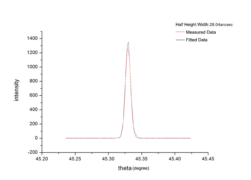
1)Typical X-Ray Diffraction (XRD) Curve of Sapphire (Al2O3) Crystals Substrates
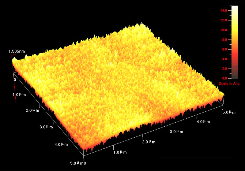
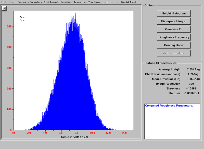
2) Typical Surface Roughness of Sapphire (Al2O3) substrate <0001> measured by Atomic Force Microscope (AFM) in 5μm x 5μm Scale

Copyright © 2012-2024 All Rights Reserved. 京ICP备01000000号 XML