
| Code | Size | Thickness | Orientation | Surface Finish | Unit Price | Delivery | Cart |
|---|---|---|---|---|---|---|---|
| 642-001 | 5x5mm | 0.5mm | <100> | SSP | Inquire | 2 weeks | |
| 642-002 | 5x5mm | 0.5mm | <100> | DSP | Inquire | 2 weeks | |
| 642-003 | 5x5mm | 0.5mm | <110> | SSP | Inquire | 2 weeks | |
| 642-004 | 5x5mm | 0.5mm | <111> | SSP | Inquire | 2 weeks | |
| 642-005 | 10x10mm | 0.5mm | <100> | SSP | Inquire | 2 weeks | |
| 642-006 | 10x10mm | 0.5mm | <100> | DSP | Inquire | 2 weeks | |
| 642-007 | 10x10mm | 0.5mm | <110> | SSP | Inquire | 2 weeks | |
| 642-008 | 10x10mm | 0.5mm | <111> | SSP | Inquire | 2 weeks | |
| 642-009 | Φ12.7mm | 0.5mm | <100> | SSP | Inquire | 2 weeks | |
| 642-010 | Φ12.7mm | 0.5mm | <100> | DSP | Inquire | 2 weeks | |
| 642-011 | Φ20mm | 0.5mm | <100> | SSP | Inquire | 2 weeks | |
| 642-012 | Φ20mm | 0.5mm | <100> | DSP | Inquire | 2 weeks | |
| 642-013 | Φ25.4mm | 0.5mm | <100> | SSP | Inquire | 2 weeks | |
| 642-014 | φ25.4mm | 0.5mm | <100> | DSP | Inquire | 2 weeks |
Strontium Titanate or SrTiO3 (STO) single crystal has a twinless crystal structure and very good physical and mechanical properties for film growth. STO provides a good lattice match to most materials with Perovskite structure. It is an excellent substrate for epitaxial growth of HTSC (High-Temperature Superconductor) and various oxide thin films. Its lattice constant (3.905Å) matches well with the common high TC superconductive material YBCO (lattice constant 3.88 Å). STO is also a suitable platform for other high TC films such as Bi-system, La-system, and others. SrTiO3 single crystal has been utilized for special optical windows and as a high-quality sputtering target as well. It can also accommodate diverse film growth technologies such as Magnet Sputtering, Pulsed Laser Deposition (PLD), Vaporization, MOCVD, CVD, laser MBE, etc. Films made with these materials and technologies on SrTiO3 wafers exhibit excellent performance.
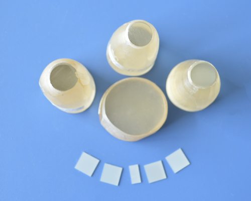
Shanghai North Optics provides stocked standard SrTiO3 (or STO) wafers and customized wafers.
Common Specifications:
| Materials | SrTiO3 crystals | Orientations | <100>,<110>,<111> |
| Orientation Error | ±0.5° | Maximum Diameter | 35mm |
| Typical Thickness | 0.5mm, 1.0mm | Thickness Tolerance | ±0.05mm |
| Size Tolerance | ±0.1mm | Surface Finish | SSP or DSP |
| Roughness | Ra<0.5nm | Cleanness and Package | class 1000 clean room, class 100 bags |
STO Basic Properties:
| Crystal Structure | M6 | Growth Method | Blaze method |
| Unit Cell Constant | a=3.905Å | Twin Structure | Twin free |
| Color | Colorless to light yellow | Melt Point(℃) | 2080 |
| Density(g/cm3) | 5.175(g/cm3) | Hardness | 6-6.5(mohs) |
| Thermal Expansion(/℃) | 9.4×10⁻⁶ | Thermal Conductivity | 120 milliwatts/cm °C at 100 °C |
| Dielectric Constants | ε=300 | Chemical Stability | Insoluble in water |
| Tangent Loss | ~5×10⁻⁴(300k) ~3×10⁻⁴(77k) | Specific Resistivity | > 107Ohm/cm |
| Transmission Range | 0.4 to 6 µm | Refraction Index | nc = 2.380 nd = 2.409 nf = 2.488 |
| Dispersion | (nf - nc) = 0.108 |
Curves:
1)Typical X-Ray Diffraction (XRD) Curve of SrTiO3 Crystals Substrates

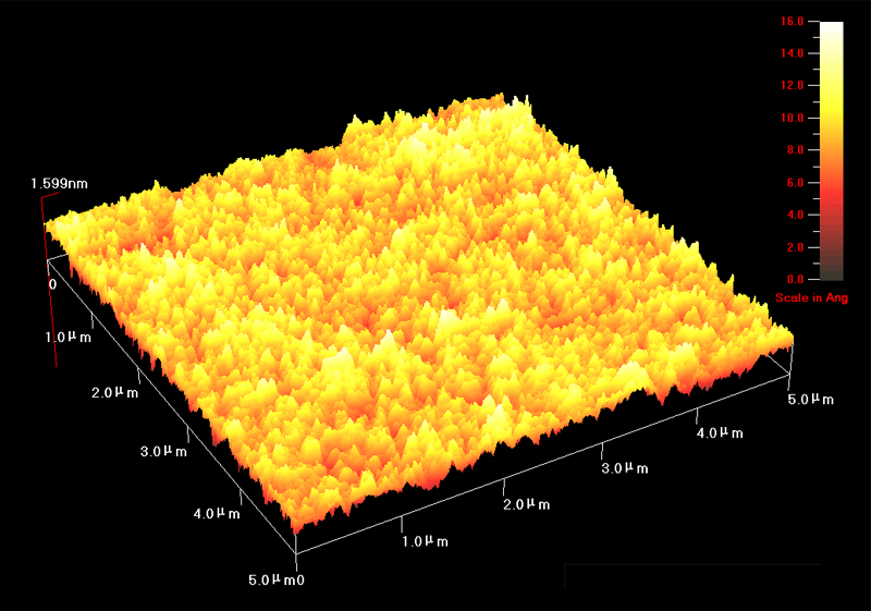
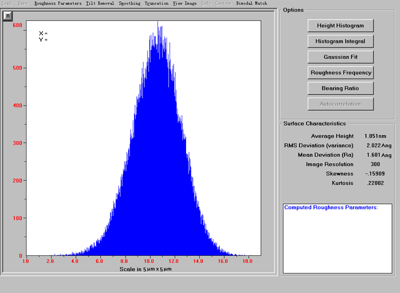
2) Typical Surface Roughness of SrTiO3 substrate <100> measured by Atomic Force Microscope (AFM) in 5μm x 5μm Scale

Copyright © 2012-2024 All Rights Reserved. 京ICP备01000000号 XML